Archived: the original hand-wired prototype. The current build uses the C5 PCB. Go to the C5 guide →

A DIY build guide

Build your own Codex Micro.

I wanted the OpenAI × Work Louder keypad, but it was unavailable. So I put together a guide to making my own version, with the files and steps for anyone who wants to do the same.

Print the enclosure, gather the electronics, and see how every piece fits. This is an independent DIY recreation; the original design belongs to OpenAI and Work Louder.

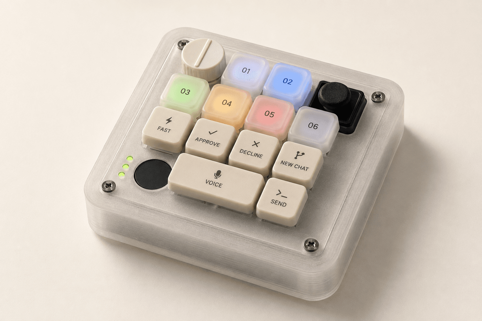
Concept render of the DIY Codex Micro: translucent case, six numbered illuminated agent keys, and labeled Fast, Approve, Decline, New Chat, Voice, and Send keys.
Concept render · DIY prototype with functional key labels. Use the CAD and fit checks for dimensions.

Before you start

Choose your electronics route before ordering or printing. This is a DIY prototype; full native Codex behavior requires genuine compatible electronics.

OpenAI explicitly lists Creator Micro 2 as compatible. The model with Bluetooth is the Pro; the Base is wired. A verified OEM PCB-only kit was not found. If matching the original is the priority, start with a complete genuine unit, verify it works, and customize its enclosure only after measuring it. OpenAI compatibility guide ↗ · Manufacturer specifications ↗

Recommended for your requirement

Native electronics + printed exterior

Retain the factory controller, LEDs, touch electrode, switch assembly, firmware, diffuser, and—on Pro—the original battery and charging circuit. That preserves the supported connection to Codex.

What still needs work: measure the donor PCB, mounting holes, connectors, antenna and diffuser; then revise the case. No donor-compatible enclosure is claimed in this package.

Creator Micro 2 Pro ↗ · Codex Micro ↗

Availability: Codex Micro page showed out of stock ($230). Creator Micro 2 page showed “Not available” without a price. Confirm the selected variant at purchase; no order was placed.
Prototype / additional development

Custom electronics + supplied CAD

USB-C KB2040, hand-wired switches, planar joystick, rotary encoder, capacitive touch, six key LEDs and eight perimeter LEDs. The files below form a buildable prototype design, subject to physical fit and electrical testing.

Included software: USB function keys, dial scroll, joystick arrows, three touch-selected banks, and individually addressable RGBW lights.

Missing for parity: native detection, automatic task status, task switching, voice behavior, reasoning control, app settings, and Bluetooth.

Custom electronics are not a substitute purchase for the full-function donor route.

Feature acceptance matrix

RequirementGenuine supported unitIncluded custom prototype
Native device setup and remappingDocumentedNot implemented
Six task-linked colors and selected-key pulseDocumentedLED hardware; manual color commands only
Task switching, approve / decline / sendDocumentedGeneric F13–F24 keys; app bindings still needed
Push-to-talk and recording / processing lightsDocumentedNot implemented; no microphone in the keypad
Reasoning and composer dial modesDocumentedScroll + Enter only
Joystick actions and touch inputDocumentedArrows + three banks
Bluetooth and rechargeable batteryCodex Micro / Creator Micro 2 ProNot included in USB design
OEM case proportions, finish and feelFactory productPhoto reconstruction; deeper hand-wired body

Native behavior source: OpenAI’s current setup documentation. Color and behavior changes in future app releases must be tested on the running app. These are separate from the geometry checks performed here.

Parts checklist

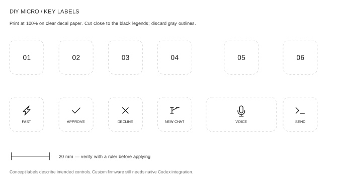
Check off what you have. Open print files or go straight to the supplier.

0 items checkedLoading your checklist…

Make these on your 3D printer.

Print checklist. Check off parts you have. Click a part name for print files.
#HavePartMaterialQuantityGet it
1Clear PETG1
2White PETG1
3White PETG1
4Black PETG1 adapter + 1 corner test
5Black PETG1
6White PETG1
7Black PETG1 tray
8Clear PETG6
9White PETG5
10White PETG1
11White PETG1 test piece
12Clear PETG1 test piece

Buy31 items

Electronics, hardware, materials, and donor options.

Buy checklist. Check off parts you have. Part names open supplier links in a new tab.
#HavePartTypeQuantityGet it
13Adafruit KB2040Electronics1Buy ↗
14Gateron North Pole Yellow 2.0Electronics13Buy ↗
15Thumb slide joystickElectronics1Buy ↗
16Rotary encoder with push switchElectronics1Buy ↗
17Encoder nut and washerHardware1 setBuy ↗
18Mini RGBW NeoPixel boardElectronics14Buy ↗
1974AHCT125 level shifterElectronics1Buy ↗
201N4148 signal diodeElectronics13Buy ↗
21Silicone hookup wireElectronicsAs neededBuy ↗
22Copper touch electrodeElectronics1 diskBuy ↗
233 mm indicator LEDElectronics3Buy ↗
24Resistors and capacitorsElectronics1 small setBuy ↗
25Small prototype circuit boardElectronics1Buy ↗
26M3 heat-set insertHardware10 installed (+2 for tray sample)Buy ↗
27M3 × 8 mm plate screwHardware4Buy ↗
28Low-profile M3 × 8 mm screwHardware2Buy ↗
29Steel weight washerHardware4 optionalBuy ↗
30Adhesive rubber feetHardware4 pads or a stripBuy ↗
31USB-C data cableHardware1Buy ↗
32Insulation and mounting tapeHardwareAs neededBuy ↗
33LED mounting tape — 3M 9474LEHardware1 pack of 5 sheetsBuy ↗
34Clear key-label decal paperHardwarePart of one sheetBuy ↗
35Clear PETGMaterialsAbout 150 gBuy ↗
36White PETGMaterialsAbout 100 gBuy ↗
37Black PETGMaterialsAbout 50 gBuy ↗
38Creator Micro 2 ProNative1 donor optionBuy ↗
39Genuine Codex MicroNative1 alternativeBuy ↗
40Frosted MX Pure capsNative6 × 1UBuy ↗
41Joystick M1.6 × 10 mm screws — v5Hardware2Buy ↗
42Joystick M1.6 hex nutsHardware2Buy ↗
43Baffle tray screws — reuse M3 × 8 mmHardware4 spare (2 reused from sample)Buy ↗

Choose either custom electronics or a genuine donor route. Supplier availability and prices can change. Generic hardware links require selecting the stated dimensions.

3D printing

These materials have different jobs. Use the material listed beside each printed part.

Flat keycaps · updated 13 September 2026: Both cap files now have flat finger surfaces, rounded corners and a 0.5 mm beveled rim. File 08 serves the white command caps and clear agent caps; file 09 is the white wide cap. Print the top facing up at 100% scale. Start with 0.10–0.12 mm layers on a 0.4 mm nozzle; support the underside as needed and keep the cross sockets clear. Print a stem-fit coupon and one cap before the full set. Physical fit and finish still need a test print.

Buy colorless clear / natural PETG for light transmission. Use opaque white and black where light should be reflected or blocked.

Light transmission

Clear / natural PETG

Print the case and six agent keycaps. Its 0.8 mm perimeter windows let the LED colors escape. Clear plate printing is optional for a more translucent appearance.

Allow roughly 150 g for these parts plus trials. Printed layers usually make clear filament look frosted; the actual result depends on settings and thickness.

PETG · choose Clear ↗
Visible opaque parts

White PETG

Print the structural plate, five individual command caps, wide cap, dial and foot. Ordinary white is appropriate here; it is not a replacement for clear agent caps.

Allow roughly 100 g. Purchasing molded keycaps gives smoother surfaces and more reliable stem fit.

PETG · choose White ↗
Light isolation

Black PETG

Print one six-light baffle tray and the touch cap, after the two-key sample fits. The v5 joystick corner and separate adapter can use existing PETG in any color; follow their different support settings in the v5 guide. The baffles keep one agent’s light from spilling into the next.

Allow roughly 50 g. Use black PETG for the new screw-fastened tray. Use adhesive rubber feet; TPU is optional, not required.

PETG · choose Black ↗

These are material allowances, not slicer weight estimates. Three new spools may cost about $55–85, while this build uses only a fraction of each. Confirm 1.75 mm versus 2.85 mm for your printer before ordering; the links default to 1.75 mm.

For faithful colors: choose colorless filament. Tinted blue, gray, smoke, glitter and fiber-filled plastics change or block the light. Sand a test patch lightly for diffusion. Neither FDM PETG nor a printed keycap will exactly reproduce CNC-sandblasted polycarbonate or molded PBT. For the donor route, retain the factory lightpipe and use six frosted MX Pure caps; the vendor listed those as a pre-order.

Starting print profile

SettingStarting pointReason / constraint
Nozzle / layer height0.4 mm / 0.20 mmUse 0.10–0.12 mm for keycaps and 0.12–0.16 mm for the dial; 0.2 mm nozzle improves sockets if available.
Walls / top & bottom4 perimeters / 5 layersUse local solid modifiers around insert bosses and switch lands.
Infill20–30% for opaque partsPerimeter windows are modeled thin. Do not use sparse infill inside an optical window.
TemperatureFilament’s own PETG presetPolymaker lists 240–260°C nozzle and 60–70°C bed; start within your printer’s supported range.
Moisture / plateDry filament; suitable release layerFollow spool instructions. PETG can bond too strongly to smooth PEI or glass.
Bed sizeAt least 120 × 120 mm for one caseLargest part is 110 × 110 mm; allow for brim and actual printable area.
Scale100%, millimetresAdjust socket/cutout parameters instead of scaling the entire model.

Filament guidance: Polymaker PETG specifications. Actual printer model, nozzle and calibrated tolerances remain unconfirmed.

Assembly

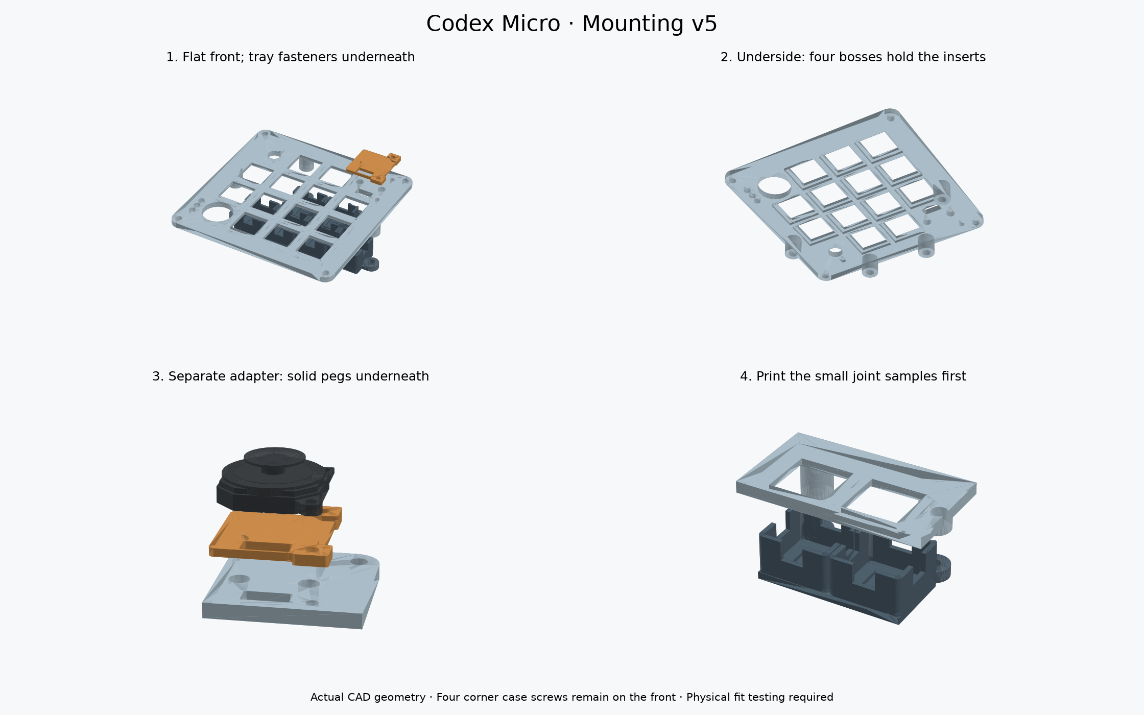
Mounting v5 adds hidden tray screws and a separate pegged joystick adapter. Print the four small fit pieces before the full plates. Open the current interactive CAD guide ↗

The original keyboard animation below shows older mounts and adhesive baffles. Use the v5 guide for the new mechanical assembly.

Click a part for print files or buying links.Loading 3D model…

Build it, one step at a time.

Choose a step to see its parts, learn the idea behind it, and check your work. These lessons follow the custom build using the supplied Rev A files.

Step 01 / 10

Print the fit samples

Learn how print tolerances affect a real fit.

Test the switch aperture, MX socket and insert fit before printing the body01 / SWITCH APERTURE14.0 mm14.1 mm14.2 mmChoose the aperture that lets the real switch latch.02 / STEM + INSERTMX socketGrip, no split.M3 insertStraight, no spin.
Fit-test schematic, not to scale. These samples are test pieces and stay out of the finished keyboard.
On your bench
Gateron North Pole Yellow 2.0 M3 heat-set insert

How to do it

  1. Print the switch-fit coupon (file 10) and stem/insert coupon (file 11), using the materials and settings you intend to use for the finished parts.
  2. Try a real MX switch in the 14.0, 14.1 and 14.2 mm apertures. Choose the fit that clips in securely without forcing or cracking the plastic.
  3. Test the MX stem socket and one specified M3 insert in the second coupon. If the fit is wrong, adjust the CAD parameters, regenerate and repeat before printing the full set.

Why it matters

A printer does not reproduce every hole at its exact CAD size. Material, extrusion and cooling affect the fit. A small coupon lets you calibrate the mating surfaces using little filament, before committing to the whole case.

Before you move on

The switch clips in and stays seated; the keycap socket grips without splitting; the cooled insert stays straight and does not spin.

Step 1 of 10
Using genuine donor electronics?

Native route: preserve the working assembly

  1. Connect a genuine unit in its original case and complete the official setup. Confirm task colors and controls before changing hardware.
  2. Measure with the donor worksheet. If opening a Pro unit, unplug USB, turn it off and disconnect the battery before moving the board. Keep its original charger, protection circuit and cell together.
  3. Revise and test-print the mounting interface. Retain the factory switch/LED assembly and lightpipe. Provide access to USB and the rear button, clearance around the antenna, and a measured gap at the touch electrode.
  4. Fit the revised shell without loading the PCB or pinching wires. Reconnect the original components and run the acceptance checklist below. The supplied custom-PCB-free case is not approved for this transplant.

Mounting v5: the lower tray screws upward into inserts underneath the upper plate. The joystick sits on a separate pegged adapter with raised tab supports; M1.6 × 10 screws pass down into exposed nuts. Print the four small test pieces first. Both full plates change. Current CAD and fit guide. The original keyboard animation shows older mechanical parts.

Prototype fit checks that need the actual partsThe slide joystick has no controlled supplier drawing; use the new screw-retained fit sample and its guide. Keycap sockets depend on printer calibration. At full key travel, caps must clear the plate and each other. The dial must rotate freely and still depress. LED solder joints must not touch switch pins. No physical print or electrical bench test has been performed here.

Matrix: view from above, USB at the rear

Row / GPIOC1 / D6C2 / D7C3 / D8C4 / D9
R1 / D2Encoder, separate wiringAgent 01Agent 02Joystick, separate wiring
R2 / D3Agent 03Agent 04Agent 05Agent 06
R3 / D4Command 1Command 2Command 3Command 4
R4 / D5Touch, separate wiringWide key / left switchWide key / right switchCommand 6

When soldering from underneath, this layout is mirrored left-to-right. Label rows and columns before flipping the plate.

Electrical connection map

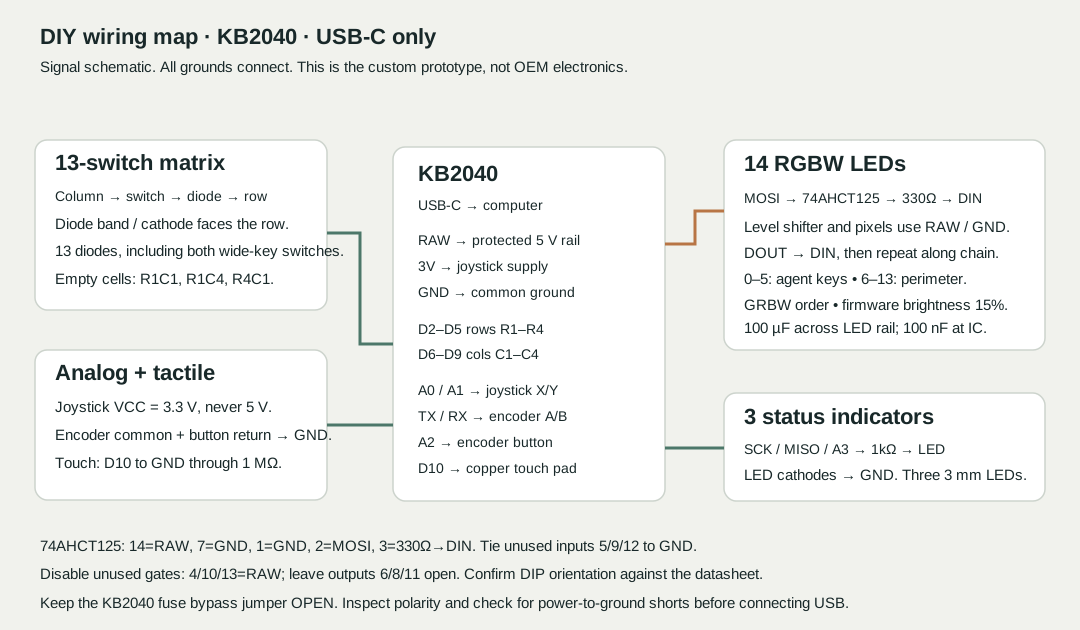
DIY wiring map · KB2040 · USB-C onlySignal schematic. All grounds connect. This is the custom prototype, not OEM electronics. KB2040 USB-C → computerRAW → protected 5 V rail3V → joystick supplyGND → common groundD2–D5 rows R1–R4D6–D9 cols C1–C4A0 / A1 → joystick X/YTX / RX → encoder A/BA2 → encoder buttonD10 → copper touch pad 13-switch matrixColumn → switch → diode → rowDiode band / cathode faces the row.13 diodes, including both wide-key switches.Empty cells: R1C1, R1C4, R4C1. Analog + tactileJoystick VCC = 3.3 V, never 5 V.Encoder common + button return → GND.Touch: D10 to GND through 1 MΩ. 14 RGBW LEDsMOSI → 74AHCT125 → 330Ω → DINLevel shifter and pixels use RAW / GND.DOUT → DIN, then repeat along chain.0–5: agent keys • 6–13: perimeter.GRBW order • firmware brightness 15%.100 µF across LED rail; 100 nF at IC. 3 status indicatorsSCK / MISO / A3 → 1kΩ → LEDLED cathodes → GND. Three 3 mm LEDs. 74AHCT125: 14=RAW, 7=GND, 1=GND, 2=MOSI, 3=330Ω→DIN. Tie unused inputs 5/9/12 to GND. Disable unused gates: 4/10/13=RAW; leave outputs 6/8/11 open. Confirm DIP orientation against the datasheet. Keep the KB2040 fuse bypass jumper OPEN. Inspect polarity and check for power-to-ground shorts before connecting USB.

Keep power domains correct

Power pixels and the 74AHCT125 from the KB2040’s fused RAW rail. Power the joystick from 3V so its analog outputs stay within 3.3 V. All grounds join. Leave the fuse-bypass jumper open.

Budget estimate: 14 × 75 mA × 15% ≈ 158 mA for the LEDs at the worst RGBW setting, plus board and indicators. Target under 250 mA total and verify with a USB meter. This is an estimate, not a measured result.

Put a 100 µF / ≥10 V capacitor across the LED rail and 100 nF close to the shifter’s supply pins. Do not add an external supply to this USB-powered build.

Joystick and encoder pinout

On SparkFun’s COM-09426, the bottom-view pad sequence is X, VCC, Y, GND; GND is nearest the two mounting tabs. Use the linked seller’s orientation diagram and a meter—other PSP replacements may differ. Despite the seller’s Arduino example, this build uses 3.3 V VCC.

Encoder A/B go to TX/RX and common to GND. Its separate switch goes between A2 and GND. If turn direction is reversed, swap A/B in firmware. No resistor is needed for the encoder switch because the firmware enables its pull-up.

Electrical sources: KB2040 pinout · LED level shifting · Joystick · Encoder drawing.

Wire it together

One small circuit at a time. Start with the knob, build the LED circuit on the perfboard, then light one key. These are the short steps from our workbench walkthrough, with a reason and a checkpoint for each.

0 of 36 checkpoints complete. Saved in this browser on this device.

New to soldering? Read this first.

USB stays unplugged while you solder or move wires. Power on only at the test checkpoints. A soldering iron holder, ventilation and eye protection make the work easier and safer.

A ribbon cable is several insulated wires joined side by side. Peel apart the conductors you need without nicking the insulation. Strip only the ends. Four inches is about 10 cm; 3 mm is roughly ⅛ inch.

Hold the part, not the hot joint. Use a small vise, helping hands, or heat-resistant tape on a soldering surface. Tin the pad and wire, bring them together, then briefly heat both. Keep still as the joint cools.

Perfboard holes are separate. An insulated wire goes across the top. Underneath, its bare end bends to the target pad or chip leg. Solder both contacts. Use the bare wire to span the gap rather than a large solder blob. Trim only the leftover tail; hold the offcut as you clip.

Ground is a shared connection. G and GND on the KB2040 are the same ground. A4 on the perfboard means column A, row 04; it is not a KB2040 pin name. The underside is mirrored, so locate holes from the top before flipping the board.

These soldered connections can stay in the finished build, but wire lengths, insulation and enclosure fit must be checked before fastening the plate. Printed mounts remain prototypes.

01

Get the KB2040 ready

Start with the controller alone. No switches or LEDs need to be connected yet.

Have ready KB2040, a USB data cable, your computer.

Make the board appear in Finder

01Install CircuitPython
  1. If CIRCUITPY already appears when you plug in, skip this step. Back up an existing code.py before replacing it.
  2. Download the CircuitPython UF2 specifically for Adafruit KB2040. With USB unplugged, hold BOOT, plug USB in, then release BOOT when RPI-RP2 appears.
  3. Copy the UF2 onto RPI-RP2. It disappears and comes back as CIRCUITPY. Quit macOS Keyboard Setup Assistant if it opens; our small keypad cannot complete the normal full-keyboard identification steps.
Why

CircuitPython is the software that runs our small Python programs on the board.

Check

CIRCUITPY is visible. RPI-RP2 is the installer drive; CIRCUITPY is where code.py goes.

02Add the keyboard library
  1. Open CIRCUITPY/boot_out.txt to check the CircuitPython major version. Download the matching Adafruit CircuitPython library bundle.
  2. Create a lib folder on CIRCUITPY if it does not exist. Copy the entire adafruit_hid folder from the bundle into CIRCUITPY/lib.
  3. Each test below is a replacement code.py, not an extra program to run alongside the old one. Keep a backup on your computer. Install only the stage you are testing.
Why

The HID library lets the KB2040 send normal keyboard presses to your computer.

Check

You have CIRCUITPY/lib/adafruit_hid. Do not put code.py in lib.

Next: Make the knob click ↓
02

Make the knob click

The knob is two controls in one: a pushbutton and a rotation sensor. Test the button first.

Have ready Encoder, two insulated wires, soldering iron, solder, wire stripper, a holder or heat-resistant tape.

GA2GA2OuterMiddleOuterUNDERSIDE
Two-terminal side: the pushbutton. The pictured terminal order may be swapped; the button has no polarity. Match the terminal groups, not the orientation of the knob cap.

Two wires, one keypress

01Find the two button terminals
  1. Unplug USB. Look at the underside of the Adafruit 377 encoder: one side has TWO electrical terminals, and the other has THREE.
  2. The two-terminal side is the pushbutton. The three-terminal side measures rotation. Large metal mounting tabs are not signal terminals.
  3. Cut two wires roughly 4 inches (10 cm) long, or longer if your case layout needs it. Strip about 3 mm at each end. Leave enough slack to lift the plate.
Why

Pressing the knob joins the two button terminals, like closing a tiny door.

Check

You are using the two-terminal side. This step does not require a key switch or a diode.

02Solder the button wires to the KB2040
  1. With USB unplugged, put one wire through the KB2040 pad marked G and the other through A2.
  2. Route the insulated wires from the component side and solder the pad and wire together on the underside. Either entry direction works electrically, but check clearance before mounting.
  3. A small joint should join the wire and the metal ring without touching the next ring. Trim excess wire, leaving the joint intact.
Why

A2 listens for the button; G provides ground.

Check

Trace each wire back to the printed label. A2 is not the perfboard hole A2.

03Attach those wires to the encoder
  1. Lightly tin the two button terminals and wire ends. Secure the encoder so you do not have to hold it near the iron.
  2. Solder the G wire to one of the TWO button terminals and the A2 wire to the other. Either terminal order works.
  3. The bare wire rests against the outside of the terminal; there is no slot to thread it through. Keep the two joints separate and insulate exposed joins before final assembly.
Why

A button press connects A2 to ground. The program detects that change.

Check

No bare strands touch the other terminal or the encoder metal shell.

04Test: pressing the knob types “a”
  1. Set the board on a dry nonmetal surface, inspect the joints, and plug USB in.
  2. Download button-test.py below. Back up the existing code.py, then copy the test to the root of CIRCUITPY and name it exactly code.py.
  3. Open a blank text document and click inside it. Press and release the knob once. You should see one a.
Why

This checks the controller, USB, program and your first two soldered wires together.

Check

One press produces one a. If not, confirm the file name, HID library, focused text field and the G/A2 wires before adding more parts.

Next: Make the knob turn ↓
03

Make the knob turn

Keep the working button connected. Add three wires for rotation.

Have ready The same encoder, three more insulated wires, your working button test.

TXRXGNDButtonButtonTXGNDRXUNDERSIDE
Three-terminal side: ground in the middle, TX and RX on the outside. Reversed rotation is corrected in software. Match the terminal groups, not the orientation of the knob cap.

Read left and right

01Connect the middle rotation terminal to ground
  1. Unplug USB. Cut three wires about 4 inches long. Strip about 3 mm at the ends.
  2. Use the middle terminal on the THREE-terminal side of the encoder. Connect it to a KB2040 pad labeled GND.
  3. G and GND are the same electrical ground. If your board has two holes under the GND label, either is ground. Use a free one; do not force multiple wires into an occupied hole.
Why

The center terminal is the common connection shared by both rotation signals.

Check

Ground goes to the middle of the three rotation terminals, not the middle of the encoder body.

02Connect the two outer rotation terminals
  1. Connect one outer terminal to KB2040 TX and the other to RX. Solder one connection at a time.
  2. Either outer-terminal order can be used; it changes which direction counts as clockwise in software.
  3. Keep these wires clear of the two button terminals. Leave the existing A2 button connection in place.
Why

The two signals change in a different order depending on which way you turn the knob.

Check

Three rotation wires: outer to TX, middle to GND, other outer to RX.

03Test: turning prints “r” and “l”
  1. Inspect the joints, then plug USB in. Replace code.py with knob-test.py, renamed code.py.
  2. In a blank text document, turn one click right, then one click left. The test should type r and l. Pressing still types a.
  3. If right prints l, change REVERSE_ROTATION from True to False, or the reverse, in code.py and save. You do not need to resolder the outer wires.
Why

This proves the rotation circuit works before assigning app shortcuts.

Check

The knob responds in both directions. Remember your REVERSE_ROTATION setting for the next program.

04Optional: make the knob send app shortcuts
  1. Once rotation works, reasoning-knob.py sends Control+Option+Command+Up or Down. Keep your calibrated REVERSE_ROTATION value.
  2. An app or an OS shortcut tool must actually bind those chords to increase/decrease reasoning. Availability depends on the app and its current controls.
  3. This firmware sends keystrokes only. It does not read the app’s reasoning level, and it does not create a missing app command.
Why

The physical knob can be reused for different actions by changing software.

Check

Verify the shortcut with your ordinary keyboard first, then try the knob with that app focused.

Next: Build the LED perfboard ↓
04

Build the LED perfboard

This is the same hole-by-hole layout from our bench walkthrough. Work with USB unplugged until the power-on checkpoint.

Have ready 4 × 6 cm isolated-pad perfboard (A–T / 01–14), SN74AHCT125N DIP-14, one RGBW NeoPixel, 330 Ω resistor, 104 / 100 nF capacitor, insulated wire.

Understand what you’re connecting

Open diagram ↗

All coordinates use the same top view. Solid lines are insulated wires; dashed links show the soldered connections underneath. The chip’s legs are numbered separately from the perfboard holes.

Prefer paper? Open the six-page PDF ↗

A. Prepare the LED and place the chip

01Solder three wires to the LED’s input side
  1. Look at the back of the Adafruit 4776 RGBW mini LED. Find + / 5V, GND / −, and DIN. DIN is on the side where the arrows start; do not use DOUT.
  2. With the arrows pointing right and 5V at the top, the input-side pads are top: 5V, middle: DIN, bottom: GND. If your board markings differ, follow its labels rather than this orientation.
  3. Cut three wires long enough to reach beneath the key, roughly 4 inches for our test. Strip about 2 mm at the LED ends. Tape the LED edges to a heat-resistant surface, tin the pads and ends, then briefly reheat each pair together.
  4. Label the far ends 5V, DIN and GND. Keep them disconnected for now.
Why

The switch itself is not a lamp. This separate LED shines up through the clear switch and keycap.

Check

Three separate input-side joints. No solder bridges between pads. The other three pads are for the next LED.

02Place the level shifter in D and G
  1. Orient the perfboard with A–T across the top and row 01 at the bottom. The diagrams show the used area A–K, rows 03–12.
  2. Place the chip writing-side up, with its semicircular notch pointing toward the column letters.
  3. Left legs: D10, D09, D08, D07, D06, D05, D04. Right legs: G10, G09, G08, G07, G06, G05, G04. Columns E and F sit underneath the body. Do not force the legs.
Why

The notch identifies the numbering: pin 1 is D10, pin 7 is D4, and pin 14 is G10.

Check

This coordinate plan requires separate metal pads, not a breadboard or stripboard with connected rows.

03Solder the chip in place
  1. Secure the body with tape, flip the board, and solder opposite corner legs D10 and G04 first. Remember the layout is mirrored underneath.
  2. Check that the chip is seated and oriented correctly, then solder the other 12 legs.
  3. Touch the iron to both the leg and its pad, feed in a little solder, remove the solder, then the iron. Keep each ring separate from neighboring rings.
Why

These joints hold the chip to individual pads. The next wires will connect selected pads together.

Check

All 14 legs have their own joints. No unintended bridges. Read coordinates from the top, not by counting left-to-right on the underside.

B. Ground, power and the small capacitor

01Enable the channel we will use
  1. Unplug USB. Cut a 1 inch insulated wire and strip about 4 mm from each end.
  2. From the TOP of the perfboard, put its ends through C10 and C4.
  3. Underneath, bend the bare ends to touch D10 and D4, respectively. Solder each end to its own pad and the connection it touches.
Why

Grounding enable pin 1 switches this channel on. Pin 7 is the chip ground.

Check

Only C10-D10 and C4-D4 are joined; the insulated wire connects the two ends.

02Add the loose ground lead at B4
  1. Cut a 4-inch wire. Strip about 4 mm at one end and insert it through B4 from the top.
  2. Underneath, bend that bare end to touch the existing C4 connection. Solder B4 and the join to C4.
  3. Label the free end GND. Leave it disconnected.
Why

This lead will connect the whole ground network to the KB2040.

Check

The ground path is B4-C4-D4, with the C4-C10 jumper reaching D10.

03Add the loose power lead at H10
  1. Cut a 4-inch wire. Strip about 4 mm at one end and insert it through H10.
  2. Underneath, join it to the neighboring chip leg at G10. Label its loose end 5V and leave that end disconnected.
Why

G10 is chip pin 14, its power supply.

Check

H10-G10 is separate from G9 and H9.

04Add the 104 capacitor
  1. Find the small ceramic capacitor marked 104, 100 nF or 0.1 µF. These mean the same value. It has no positive or negative leg.
  2. Put its legs through D11 and G11. The holes are 7.6 mm apart. Support each leg near the body and gently bend farther down; do not pull against the yellow body. It may sit slightly raised.
  3. Underneath, join D11 to D10 and G11 to G10. Solder each leg to its own pad and neighboring chip leg. Trim excess tails after soldering.
Why

It is a tiny energy cushion across power and ground, smoothing brief disturbances.

Check

Do not connect its two legs with bare wire. The capacitor itself is the component between the two networks.

C. Give the LED its data, ground and power

01Add the loose DATA IN lead at C9
  1. Cut a 4-inch wire. Strip about 4 mm at one end, insert it through C9 and join it to D9 underneath.
  2. Label the free end DATA IN and leave it disconnected. Keep D9 separate from grounded D10.
Why

D9 is input pin 2. It will receive the KB2040’s color instructions.

Check

C9-D9 is its own signal connection.

02Fit and solder the 330 Ω resistor
  1. Bend the resistor legs gently and insert them through B8 and B12 from the top. Either direction is correct. Leave the body slightly raised.
  2. Underneath, bend the B8 leg across C8 until it touches D8. Solder to B8 and the chip leg D8. Contact with C8 on that same row is okay.
  3. Solder the other leg to B12 only. Keep row 8 clear of rows 7 and 9. Trim tails beyond the finished joints.
Why

The resistor sits in the data path and helps protect the LED’s input.

Check

B8 connects to D8; the resistor body connects B8 to B12. Do not bypass the resistor with a wire.

03Attach the LED’s DIN wire at A12
  1. Trace the wire back to the LED’s DIN pad. Strip about 4 mm from its loose end.
  2. Insert it through A12, bend it toward the resistor leg at B12 underneath, and solder A12 and the B12 join.
  3. Trim only excess metal beyond the joined section. Leave enough insulated wire to reach the key position.
Why

The route is chip output D8 → resistor → A12 → LED DIN. This connection can stay in the final build.

Check

DIN is not DOUT, 5V or ground.

04Attach the LED’s GND wire at A4
  1. Trace the LED’s GND / − wire. Strip about 4 mm from the loose end and insert it through A4.
  2. Underneath, join A4 to the existing ground connection at B4. Solder both.
Why

The LED and chip need the same ground reference.

Check

A4-B4-C4-D4 is connected; unrelated adjacent rows remain separate.

05Attach the LED’s 5V wire at I10
  1. Trace the LED’s 5V / + wire. Strip about 4 mm and insert it through I10 (letter I).
  2. Underneath, join I10 to H10 and solder. Keep USB unplugged.
Why

The LED gets its power directly from the power network, not through the data resistor.

Check

I10-H10-G10 is one power network. We still need to finish the unused chip inputs.

D. Keep the three spare channels quiet

01Ground the first unused input
  1. Unplug USB. Cut a 1 inch insulated wire and strip about 4 mm from each end.
  2. From the TOP of the perfboard, put its ends through C6 and B5.
  3. Underneath, bend the bare ends to touch D6 and B4, respectively. Solder each end to its own pad and the connection it touches.
Why

The chip has four channels. Ground holds an unused input steady instead of letting it pick up noise.

Check

C6-D6 joins B5-B4 through the insulated wire.

02Join the other two unused inputs
  1. Unplug USB. Cut a 1 inch insulated wire and strip about 4 mm from each end.
  2. From the TOP of the perfboard, put its ends through H5 and H8.
  3. Underneath, bend the bare ends to touch G5 and G8, respectively. Solder each end to its own pad and the connection it touches.
Why

This joins unused input pins 9 and 12.

Check

This pair is not grounded until the next step.

03Connect that pair to ground
  1. Unplug USB. Cut a 1½-inch insulated wire and strip about 4 mm from each end.
  2. From the TOP of the perfboard, put its ends through I5 and A5.
  3. Underneath, bend the bare ends to touch H5 and A4, respectively. Solder each end to its own pad and the connection it touches.
Why

This gives both inputs a path to the shared ground.

Check

All three unused inputs, pins 5, 9 and 12, now reach ground.

04Join two unused enable pins
  1. Unplug USB. Cut a 1 inch insulated wire and strip about 4 mm from each end.
  2. From the TOP of the perfboard, put its ends through H6 and H9.
  3. Underneath, bend the bare ends to touch G6 and G9, respectively. Solder each end to its own pad and the connection it touches.
Why

These control whether the spare channels are on. They will go to 5V to switch them OFF.

Check

Keep these joints separate from the ground connections at H5 and H8.

05Connect those enable pins to 5V
  1. Unplug USB. Cut a 1 inch insulated wire and strip about 4 mm from each end.
  2. From the TOP of the perfboard, put its ends through I9 and J10.
  3. Underneath, bend the bare ends to touch H9 and I10, respectively. Solder each end to its own pad and the connection it touches.
Why

A high voltage on these enable pins switches the two spare channels off.

Check

I9-H9 and J10-I10 are power connections, not ground.

06Switch off the last unused channel
  1. Unplug USB. Cut a 1½-inch insulated wire and strip about 4 mm from each end.
  2. From the TOP of the perfboard, put its ends through C7 and K10.
  3. Underneath, bend the bare ends to touch D7 and J10, respectively. Solder each end to its own pad and the connection it touches.
Why

This puts enable pin 4 at 5V, switching the last spare channel off.

Check

D7 must stay separate from grounded D6. Leave output pins 6 (D5), 8 (G4), and 11 (G7) unconnected.

E. Connect the completed circuit to the KB2040

01Connect DATA IN to KB2040 MO
  1. With USB unplugged, trace the loose DATA IN wire from C9-D9. Strip about 3 mm from its free end.
  2. Solder it to KB2040 MO (letter O), not MI. On the row that reads 10, MO, MI, CLK, A0, it is between 10 and MI.
Why

MO is the pin named board.MOSI in the test program.

Check

This is the loose controller lead, not the wire already going to LED DIN.

02Connect the 5V lead to RAW
  1. Trace the loose 5V wire from H10-G10. Strip about 3 mm and solder it to KB2040 RAW, near USB and beside G.
  2. Use RAW, not 3V. Leave the board’s USB power-protection jumper unchanged.
Why

RAW supplies the LED and level shifter from USB power.

Check

Do not plug in yet; the common ground must also be connected.

03Connect the ground lead; share a junction if needed
  1. Trace the loose GND wire from B4. If a KB2040 G/GND hole is free, you can solder it there and leave the knob’s ground wire in place. The ground pads are electrically shared.
  2. Our PDF shows this alternative: unplug USB, check the existing knob wire on G reaches perfboard A3 comfortably, then desolder that wire from G. Do not pull until its solder has melted.
  3. Insert the moved knob wire through A3 and join A3 to A4 underneath. Solder it. Put the loose B4 ground lead into the now-empty KB2040 G hole and solder.
  4. If that wire will not reach, use a longer insulated wire. Do not stretch a soldered connection. The other encoder ground on GND stays connected.
Why

The perfboard becomes a shared junction: knob → A3-A4 → B4 → KB2040 G. The LED shares it too.

Check

For the PDF layout, confirm BOTH the A3-A4 joint and B4-to-KB-G lead are complete. With a free GND pad, the A3 reroute is unnecessary.

04Check before applying power
  1. With USB unplugged, inspect both sides under good light. No stray strand or unintended solder bridge should join power and ground or neighboring chip legs.
  2. If you have a multimeter, check continuity of the intended paths and for a persistent near-zero resistance between power and ground. A capacitor can cause a brief changing reading; do not power a circuit with a sustained short.
  3. Without a meter, a visual inspection is only a basic check, not electrical verification. Keep the boards on a dry nonmetal surface and all loose metal clear. Stop and correct any uncertain joint.
Why

A successful code upload cannot tell us whether every solder joint is right.

Check

The map and PDF describe intended connections. They do not verify your soldered board.

Next: Light one key ↓
05

Light one key

Use one LED first. This is the point where we check the light, before committing to the baffle tray.

Have ready Completed perfboard, one RGBW LED, clear switch and keycap for the optical check.

Power on, then send a color

01Do a basic power-on check
  1. Place the inspected circuit on a dry nonmetal surface and plug the KB2040 into USB. Do not hold exposed joints against metal.
  2. Confirm CIRCUITPY appears. The external LED may remain dark until its program sends a color.
  3. Unplug immediately for a burning smell, smoke or a USB power warning. Do not keep retrying a suspected short.
Why

Power alone does not tell an addressable LED which color to display.

Check

CIRCUITPY appears. This is a controller check, not yet a successful LED test.

02Install the one-LED test
  1. The download bundle contains three staged tests, the HID folder and NeoPixel libraries. Copy its lib contents into CIRCUITPY/lib. Do not remove other libraries you already use.
  2. Back up code.py, then copy led-test.py to CIRCUITPY and rename it code.py. Keep your calibrated REVERSE_ROTATION setting.
  3. This program drives ONE RGBW LED on MO at 8% brightness. It keeps the knob’s r/l test and button a test. The external LED should glow dim pink.
Why

A single low-brightness pixel is enough to test the driver circuit and light leakage.

Check

Physically confirm the external LED lights. A log saying “color sent” only proves the program ran.

03If the LED stays dark
  1. Read the CircuitPython serial console for an exception. Missing neopixel or adafruit_pixelbuf means the libraries are not installed. Confirm the file is code.py, not code.py.txt.
  2. Unplug before checking wiring. Trace MO → C9-D9; D8 → B8 → resistor → B12-A12 → DIN. Confirm the LED input side, RAW supply and shared ground.
  3. Recheck chip notch orientation and the 104 capacitor joints. A photo cannot rule out a bad joint or hidden short; a multimeter is the next useful diagnostic tool if the cause is unclear.
Why

Troubleshoot one path at a time instead of changing many wires at once.

Check

Do not infer that the light is working merely because Finder shows CIRCUITPY.

04Compare the light with and without a baffle
  1. Unplug USB before positioning the LED below one clear switch and cap. Keep its metal pads isolated from the switch pins. Add two neighboring caps for comparison.
  2. Power it again without touching the wiring. Compare the lit key and its neighbors in normal room light, then dimmer light.
  3. Unplug, add one existing opaque baffle, then repeat. If it makes a useful difference, continue the tray fit test. If not, you can defer the extra baffle print.
Why

This small test answers whether light-blocking parts improve your actual printed keys.

Check

This is an optical test, not proof of the full tray fit. Do not move a powered LED against exposed switch pins.

Next: the remaining circuits ↓
06

Finish the remaining circuits

Get the knob and one LED working before moving on. These are the remaining wiring references, not completed bench checkpoints.

Fit-test the top plate before soldering the keys. A hand-wired switch matrix makes plate replacement a desoldering job; it is not hot-swappable.

Before adding more LEDs: plan their physical order and wire lengths. The full design has six key LEDs and eight perimeter LEDs. Add the planned bulk capacitor across the LED supply, confirm its polarity, and review the total current against the USB supply and KB2040 RAW protection. Do not simply run 14 pixels at full white or bypass the fuse.

Add the key matrix

Choose a key to see its complete column → switch → diode → row connection. Splice keys on the same row or column into that shared wire.

Key positions: viewed from above, USB at the back. Switch photo: metal legs visible.

Agent 01

D7 · column 2 → Switch → diode → D2 · row 1

Solder D7’s column wire to either metal switch leg. Join the other leg to the unbanded end of its own 1N4148 diode. Join the banded end to the D2 row wire. Insulate every exposed crossing.

Check: Before connecting the matrix to the controller, hold this key: diode mode should conduct with red on the column and black on the row, but not the reverse. Release it: the path should open.
Agent 02

D8 · column 3 → Switch → diode → D2 · row 1

Solder D8’s column wire to either metal switch leg. Join the other leg to the unbanded end of its own 1N4148 diode. Join the banded end to the D2 row wire. Insulate every exposed crossing.

Check: Before connecting the matrix to the controller, hold this key: diode mode should conduct with red on the column and black on the row, but not the reverse. Release it: the path should open.
Agent 03

D6 · column 1 → Switch → diode → D3 · row 2

Solder D6’s column wire to either metal switch leg. Join the other leg to the unbanded end of its own 1N4148 diode. Join the banded end to the D3 row wire. Insulate every exposed crossing.

Check: Before connecting the matrix to the controller, hold this key: diode mode should conduct with red on the column and black on the row, but not the reverse. Release it: the path should open.
Agent 04

D7 · column 2 → Switch → diode → D3 · row 2

Solder D7’s column wire to either metal switch leg. Join the other leg to the unbanded end of its own 1N4148 diode. Join the banded end to the D3 row wire. Insulate every exposed crossing.

Check: Before connecting the matrix to the controller, hold this key: diode mode should conduct with red on the column and black on the row, but not the reverse. Release it: the path should open.

Agent 05

D8 · column 3 → Switch → diode → D3 · row 2

Solder D8’s column wire to either metal switch leg. Join the other leg to the unbanded end of its own 1N4148 diode. Join the banded end to the D3 row wire. Insulate every exposed crossing.

Check: Before connecting the matrix to the controller, hold this key: diode mode should conduct with red on the column and black on the row, but not the reverse. Release it: the path should open.

Agent 06

D9 · column 4 → Switch → diode → D3 · row 2

Solder D9’s column wire to either metal switch leg. Join the other leg to the unbanded end of its own 1N4148 diode. Join the banded end to the D3 row wire. Insulate every exposed crossing.

Check: Before connecting the matrix to the controller, hold this key: diode mode should conduct with red on the column and black on the row, but not the reverse. Release it: the path should open.

Fast

D6 · column 1 → Switch → diode → D4 · row 3

Solder D6’s column wire to either metal switch leg. Join the other leg to the unbanded end of its own 1N4148 diode. Join the banded end to the D4 row wire. Insulate every exposed crossing.

Check: Before connecting the matrix to the controller, hold this key: diode mode should conduct with red on the column and black on the row, but not the reverse. Release it: the path should open.

Approve

D7 · column 2 → Switch → diode → D4 · row 3

Solder D7’s column wire to either metal switch leg. Join the other leg to the unbanded end of its own 1N4148 diode. Join the banded end to the D4 row wire. Insulate every exposed crossing.

Check: Before connecting the matrix to the controller, hold this key: diode mode should conduct with red on the column and black on the row, but not the reverse. Release it: the path should open.

Decline

D8 · column 3 → Switch → diode → D4 · row 3

Solder D8’s column wire to either metal switch leg. Join the other leg to the unbanded end of its own 1N4148 diode. Join the banded end to the D4 row wire. Insulate every exposed crossing.

Check: Before connecting the matrix to the controller, hold this key: diode mode should conduct with red on the column and black on the row, but not the reverse. Release it: the path should open.

New Chat

D9 · column 4 → Switch → diode → D4 · row 3

Solder D9’s column wire to either metal switch leg. Join the other leg to the unbanded end of its own 1N4148 diode. Join the banded end to the D4 row wire. Insulate every exposed crossing.

Check: Before connecting the matrix to the controller, hold this key: diode mode should conduct with red on the column and black on the row, but not the reverse. Release it: the path should open.

Voice · left

D7 · column 2 → Switch → diode → D5 · row 4

Solder D7’s column wire to either metal switch leg. Join the other leg to the unbanded end of its own 1N4148 diode. Join the banded end to the D5 row wire. Insulate every exposed crossing.

Check: Before connecting the matrix to the controller, hold this key: diode mode should conduct with red on the column and black on the row, but not the reverse. Release it: the path should open.

Voice · right

D8 · column 3 → Switch → diode → D5 · row 4

Solder D8’s column wire to either metal switch leg. Join the other leg to the unbanded end of its own 1N4148 diode. Join the banded end to the D5 row wire. Insulate every exposed crossing.

Check: Before connecting the matrix to the controller, hold this key: diode mode should conduct with red on the column and black on the row, but not the reverse. Release it: the path should open.

Send

D9 · column 4 → Switch → diode → D5 · row 4

Solder D9’s column wire to either metal switch leg. Join the other leg to the unbanded end of its own 1N4148 diode. Join the banded end to the D5 row wire. Insulate every exposed crossing.

Check: Before connecting the matrix to the controller, hold this key: diode mode should conduct with red on the column and black on the row, but not the reverse. Release it: the path should open.

Extend the LED chain

Turn each mini PCB over to expose its six solder pads. Follow the printed arrows.

Actual back-side photo. DIN above DOUT; GND left, 5V right.

Carry power to every pixel

LED +5V and GND rails → 5V and GND pads on all 14 boards

Solder +5V to each right-hand 5V pad and ground to each left-hand GND pad in this back view. The duplicated pads let you carry power onward.

Check: Orient each board by its printed DIN, DOUT, 5V and GND labels before soldering. The lit face points away from you here.

Start at pixel 0

330Ω resistor from IC pin 3 → Pixel 0 · DIN

Connect the resistor’s free end to the middle pad beside DIN on the first board. Put this pixel beneath Agent 01.

Check: DIN is the center pad in the top row of this photo. Follow the printed arrows toward DOUT.

Link data through all 14

Each pixel’s DOUT → Next pixel’s DIN

Connect pixel 0 DOUT to pixel 1 DIN, then repeat in order through pixel 13. Put 0–5 beneath Agent 01–06; put 6–13 around the perimeter. Keep the wires short.

Check: There are 13 DOUT-to-DIN links between 14 boards. Do not join all DIN pads to one signal bus.

Finish the chain

Pixel 13 · DOUT → Leave open

Power pixel 13 from the shared rails and feed its DIN from pixel 12 DOUT. Leave its DOUT pad unconnected.

Check: Test a dim moving pixel before mounting. It should visit Agent 01–06 first, then each perimeter light.

Connect the joystick

These are separate controls: the dial uses switch contacts; the joystick uses analog voltages.

Joystick: underside photo. Encoder: underside drawing, shaft away from you.

Joystick ground

KB2040 G → Joystick pad 4 · GND

On the joystick’s underside, locate the four gold contacts. Pad 4 is nearest the pair of mounting tabs at the bottom of this photo. Wire it to G.

Check: Use the COM-09426 orientation shown; other PSP-style joystick parts can differ.

Joystick power

KB2040 3V → Joystick pad 2 · VCC

Connect 3V to the second contact from the top in this underside photo. Do not use the LED’s RAW rail.

Check: Confirm pad 2 goes to 3V and has no connection to RAW.

Joystick X axis

Joystick pad 1 · X → KB2040 A0

Wire the top gold contact to A0. Tin the small pad and wire separately, then make a brief solder joint and add strain relief.

Check: With power connected after inspection, X should change when you move horizontally and stay between ground and 3.3V.

Joystick Y axis

Joystick pad 3 · Y → KB2040 A1

Wire the third gold contact from the top to A1. Route it alongside the X wire without bridging adjacent pads.

Check: Leave the joystick centered while plugging in. Check both directions before closing the case.

Add touch and bank indicators

Finish the touch sensor and the three small white indicator LEDs.

KB2040: component side. LED drawings show long + and short − leads.

Connect the touch electrode

KB2040 D10 → Copper foil electrode

Solder a thin signal wire to the copper foil electrode. Route it to D10, keeping the lead short and away from the LED power runs.

Check: Insulate the copper from the case hardware, ground wiring and nearby switch legs.

Add the touch pulldown

D10 / electrode junction → 1MΩ resistor → G

Join one end of a 1MΩ resistor to the same D10 junction; connect its other end to G. The resistor is a branch to ground, not in series with the touch lead.

Check: Verify 1MΩ, not 1kΩ. A meter should read approximately 1MΩ from the isolated electrode circuit to ground.

Bank indicator 1

KB2040 CLK → 1kΩ resistor → LED 1 anode; cathode → G

Put a separate 1kΩ resistor in series with this LED’s long anode lead. Connect its short cathode lead (the flat side of the rim) to ground. Resistor direction does not matter.

Check: This LED marks bank 1. Confirm polarity before clipping the legs; in firmware CLK is board.SCK.

Bank indicator 2

KB2040 MI → 1kΩ resistor → LED 2 anode; cathode → G

Put a separate 1kΩ resistor in series with this LED’s long anode lead. Connect its short cathode lead (the flat side of the rim) to ground. Resistor direction does not matter.

Check: This LED marks bank 2. Confirm polarity before clipping the legs; in firmware MI is board.MISO.

Bank indicator 3

KB2040 A3 → 1kΩ resistor → LED 3 anode; cathode → G

Put a separate 1kΩ resistor in series with this LED’s long anode lead. Connect its short cathode lead (the flat side of the rim) to ground. Resistor direction does not matter.

Check: This LED marks bank 3. Confirm polarity before clipping the legs; in firmware A3 is board.A3.

The full-keyboard firmware uses a different mapping from these small tests: function keys for the matrix and scrolling for the dial. Install it only after its required circuits are ready, and re-check the mappings you want.

Component references & what has been tested

The knob’s button and rotation were exercised during the bench walkthrough. The one-LED configuration ran on the KB2040, but a successful program log is not confirmation that the external LED lit. Confirm each checkpoint on your own build. The finished keyboard, LED chain and printed mounts still need full assembly testing.

The PDF and explorer document the shared-ground reroute we used at A3/A4. If you use an otherwise free KB2040 GND pad, you can leave the knob ground in place instead.

KB2040 photo: Adafruit. Encoder underside and wires are explanatory drawings; follow your component’s terminals and printed labels.

Firmware & colors

Still following the bench walkthrough? Use the staged test programs until the remaining circuits are ready. The full-keyboard firmware below expects the matrix, joystick, touch input and light chain; its dial mapping differs from the knob tests.

Native setup

Use the current desktop app, connect the genuine unit, and follow its detected-device setup. On macOS, grant the requested Input Monitoring access. Choose task assignments, controls and brightness in the device settings. Work Louder Input is optional for other-app layers.

The mic key uses the computer’s microphone. Native voice feedback uses a sea-green recording animation, followed by white processing and ready feedback.

Complete official setup and behavior reference ↗

State → agent-key color

White · idle
Blue · working
Green · completed, unread
Amber · input required
Red · error
Off · unassigned

The selected task pulses. The current guide specifies red for errors; the supply-page photography can look pink. RGB values in the illustration are approximations, not published firmware constants.

Install the custom prototype firmware

Only do this on the KB2040. These files are not compatible with the genuine Work Louder board and must not replace its firmware.

  1. Install the stable CircuitPython build for Adafruit KB2040 using its BOOT + USB bootloader procedure.
  2. From the matching CircuitPython library bundle, copy adafruit_hid/, neopixel.mpy, and adafruit_pixelbuf.mpy into CIRCUITPY/lib/.
  3. Copy boot.py, code.py, and logic.py to CIRCUITPY. Unplug/replug so the second USB serial port is enabled. Keep hands off the stick and touch pad during startup calibration.
  4. Agent and command keys output F13–F24. The touch control chooses plain, Shift, or Control banks. Map these in your shortcut utility or edit the mappings. The dial scrolls and presses Enter; the joystick sends arrows.
  5. Install Python’s pyserial on the computer and use the included helper to set individual light colors.
python -m pip install pyserial
python -m serial.tools.list_ports
# Pick the KB2040 DATA port, not its REPL/console port.
python tools/set_light.py /dev/cu.usbmodemXXXX 0 0 120 255
# Windows example: replace the device path with COM7.
# LED 0–5 = agent keys; LED 6–13 = perimeter.

The helper sends a manual color command. Seeing the right color confirms LED control, not live task synchronization. Default bank colors are not agent-status indicators.

Work remaining for custom full functionality

A host integration must obtain live task identities and lifecycle events, map six keys consistently, send status and selection updates, handle voice states, dispatch app actions, and recover after reconnects. Native settings, reasoning controls, approval actions and Bluetooth add separate work. The installed app’s Work Louder library confirms a vendor RPC connection for device events and thread lighting; the supplied generic HID firmware does not implement that connection.

No tested custom bridge or native-device emulation is included. A periodic notification script is insufficient to match the original. Completion requires tests on the actual hardware and the current desktop app. The genuine electronics route avoids this unimplemented software layer.

Final checks

Mounting v5: the lower tray screws upward into inserts underneath the upper plate. The joystick sits on a separate pegged adapter with raised tab supports; M1.6 × 10 screws pass down into exposed nuts. Print the four small test pieces first. Both full plates change. Current CAD and fit guide. The original keyboard animation shows older mechanical parts.

Completed offline

The original 11 STL files passed closed-mesh checks. The six v5 printed parts pass CAD validity and watertight-mesh checks; see the v5 validation report. Individual STEP solids pass the CAD kernel validity check. The tested assembly pairs have no material overlap. The board envelope clears the case.

Input-state tests cover the wide key’s two-switch press/release ordering, joystick dead-zone behavior and malformed color input. Firmware syntax is checked.

These tests do not establish print fit, soldering correctness, optical uniformity, key travel feel, electrical current, firmware operation on hardware, or OEM donor compatibility.

Still needed from the build

Printer model, material diameter and nozzle; choice of genuine or custom electronics; actual-part measurements; first fit coupons; assembled hardware; and end-to-end software tests.

Native functionality is documented for genuine devices, but this particular printed re-housing has not been built. The custom route’s native software parity remains unimplemented.

Bench acceptance checklist

The native column is a future physical acceptance test, not a statement that the custom firmware passes it.

Downloads

STLs are oriented for printing. STEP files are for editing and may retain assembled coordinates. Use the matching STL and its orientation notes for printing. Units are millimeters.

Complete archive (includes older revisions) ↓
Older CAD and original offline guide (archive)

These preserve earlier versions. The original full-keyboard assembly has the old joystick mount and individual baffles; use the current files above for the latest design.

Printed partQuantityFiles
Print FIRST: upper joint sample v5Visible face DOWN, bosses UP. PETG, 0.15 mm layers, supports OFF. Install two M3 × 4 inserts in these upper bosses; use two existing M3 × 8 screws from underneath.1STLSTEP
Print FIRST: lower joint sample v5Black PETG, cups UP, supports OFF. M3 × 8 screws enter upward through the short mounting shelves. Test the wired LED through the 10 × 4 mm slots.1STLSTEP
Print FIRST: joystick corner v5Flat visible face DOWN; PETG, 0.10 mm layers, supports OFF. Pair with the separate v5 adapter. Uses two M1.6 × 10 screws and exposed existing M1.6 nuts.1STLSTEP
Print FIRST / reuse: joystick adapter v5PETG, 0.10 mm layers. Pegs DOWN, ear seats UP. Support UNDER the base between pegs; keep holes and seats clear. Remove supports, check it sits flat. Reuse this tested piece in final keyboard.1STLSTEP
caseOpen side up; supports in USB tunnel only if your slicer needs them.1STLSTEP
Upper plate v5 — WAITNew v5 plate required. Visible face DOWN, underside bosses UP, supports OFF. Test both mounts first. Four tray inserts are now underneath this plate; joystick supports are on the separate adapter.1STLSTEP
Lower light tray v5 — WAITNew matching v5 lower tray. Black PETG, cups UP, supports OFF. Four existing M3 × 8 screws enter from below into the upper plate. Preserve 10 × 4 mm LED slots and wire slack. Test samples first.1STLSTEP
round footFlat bottom DOWN. Washer pockets face up; secure washers with tape before assembly.1STLSTEP
touch capVisible face DOWN. Bond 13 mm copper disk immediately beneath the 0.8 mm top skin.1STLSTEP
encoder knobSocket DOWN; short bridging above nut pocket. Trial fit the D socket before pressing fully. Adhesive optional after testing.1STLSTEP
keycap 1uFlat top, 0.5 mm beveled rim. Print 6 clear and 5 white, top UP; 0.10-0.12 mm layers with a 0.4 mm nozzle. Support underside as needed, keep sockets clear. Test one cap first.11STLSTEP
keycap 2u dual stemFlat top, 0.5 mm beveled rim; white PETG, top UP. Support underside as needed, keep sockets clear. Two MX sockets 19.05 mm apart; fits two switches, not a centered stabilizer. Test fit first.1STLSTEP
switch fit couponLeft/middle/right from top: 14.0 / 14.1 / 14.2 mm. Choose snug clip fit before full print.1STLSTEP
stem insert couponCross fits -0.05 / nominal / +0.05, then 3.9 mm insert pocket. Sockets UP for inspection.1STLSTEP

Firmware, wiring and validation files

Independent DIY reconstruction. Test each circuit and printed fit; the full assembly remains a prototype.Original reference ↗